Next Instruction Access Intent Instruction
时间:2022-03-13 22:35
Executing a Next Instruction Access Intent instruction by a computer. The processor obtains an access intent instruction indicating an access intent. The access intent is associated with an operand of a next sequential instruction. The access intent indicates usage of the operand by one or more instructions subsequent to the next sequential instruction. The computer executes the access intent instruction. The computer obtains the next sequential instruction. The computer executes the next sequential instruction, which comprises based on the access intent, adjusting one or more cache behaviors for the operand of the next sequential instruction.
BACKGROUND
The present invention relates, in general, to computer systems, and in particular, to computer system processor instruction processing functionality.
From the 1960s to the present, a type of computer system, because of its essential nature in large-scale computing power, became known as the "mainframe". This mainframe (computer) operates upon a set of principles of operation which state the architecture of the machine by describing the instructions that may be executed on the mainframe.
BRIEF SUMMARY
According to one embodiment, a method, system, and program product is provided. A computer obtains an access intent instruction indicating an access intent. The access intent is associated with an operand of a next sequential instruction. The access intent indicates usage of the operand by one or more instructions subsequent to the next sequential instruction. The computer executes the access intent instruction. The computer obtains the next sequential instruction. The computer executes the next sequential instruction. This execution comprises based on the access intent, adjusting one or more cache behaviors for the operand of the next sequential instruction.
According to one embodiment, the computer stores the access intent in an internal control register.
According to one embodiment, the access intent instruction comprises an access intent operand indicating the access intent.
According to one embodiment, the access intent instruction indicates another access intent. The another access intent is associated with another operand of the next sequential instruction. The another access intent indicates usage of the another operand by the one or more instructions subsequent to the next sequential instruction.
According to one embodiment, the access intent specifies that the operand of the next sequential instruction will be accessed by the one or more instructions subsequent to the next sequential instruction such that: the operand of the next sequential instruction will be accessed by the one or more instructions subsequent to the next sequential instruction for operand store access, the operand of the next sequential instruction will be accessed by the one or more instructions subsequent to the next sequential instruction for operand fetch access, the operand of the next sequential instruction will not be accessed by the one or more instructions subsequent to the next sequential instruction, or a combination thereof.
According to one embodiment, based on the access intent, adjusting one or more cache behaviors for the operand of the next sequential instruction further comprises based on the access intent being a first value, adjusting, by the computer, a recently used state of an accessed cache line to be at or near least recently used, and based on the access intent being a second value, not adjusting, by the computer, the recently used state of the accessed cache line to be most recently used.
According to one embodiment, based on the access intent, adjusting one or more cache behaviors for the operand of the next sequential instruction further comprises based on a cache miss and the access intent, requesting, by the computer, a cache line to be read only or exclusive from a next higher level cache.
According to one embodiment, the computer comprises a processor and a co-processor.
DETAILED DESCRIPTION
In accordance with an embodiment, a method, system, and computer program product is provided for performing cache management in mainframes, in particular, cache line (cache-line) management. Specific details concerning the principles of operations of a mainframe, for example an IBM mainframe, including instructions directed towards the mainframe can be found in the "IBM z/Architecture Principles of Operation" published August 2010, reference number SA22-7832-08, incorporated herein by reference. The term CPU and processor may be used interchangeable throughout the specification.
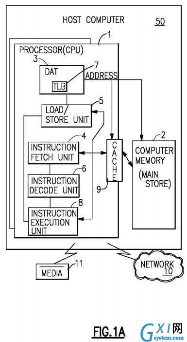
Referring to?FIG. 1A, representative components of a Host Computer system?50?are portrayed. Other arrangements of components may also be employed in a computer system, which are well known in the art. The representative Host Computer?50?comprises one or more CPUs?1?in communication with main store (Computer Memory?2) as well as I/O interfaces to storage devices?11?and networks?10?for communicating with other computers or SANs and the like. The CPU?1is compliant with an architecture having an architected instruction set and architected functionality. The CPU?1?may have Dynamic Address Translation (DAT)?3?for transforming program addresses (virtual addresses) into real address of memory. A DAT typically includes a Translation Lookaside Buffer (TLB)?7?for caching translations so that later accesses to the block of computer memory?2?do not require the delay of address translation. Typically a cache?9?is employed between Computer Memory?2?and the Processor?1. The cache?9?may be hierarchical having a large cache available to more than one CPU and smaller, faster (lower level) caches between the large cache and each CPU. In some implementations the lower level caches are split to provide separate low level caches for instruction fetching and data accesses. In an embodiment, an instruction is fetched from memory?2?by an instruction fetch unit?4?via a cache?9. The instruction is decoded in an instruction decode unit (6) and dispatched (with other instructions in some embodiments) to instruction execution units?8. Typically several execution units?8?are employed, for example an arithmetic execution unit, a floating point execution unit and a branch instruction execution unit. The instruction is executed by the execution unit, accessing operands from instruction specified registers or memory as needed. If an operand is to be accessed (loaded or stored) from memory?2, a load store unit?5typically handles the access under control of the instruction being executed. Instructions may be executed in hardware circuits or in internal microcode (firmware) or by a combination of both.
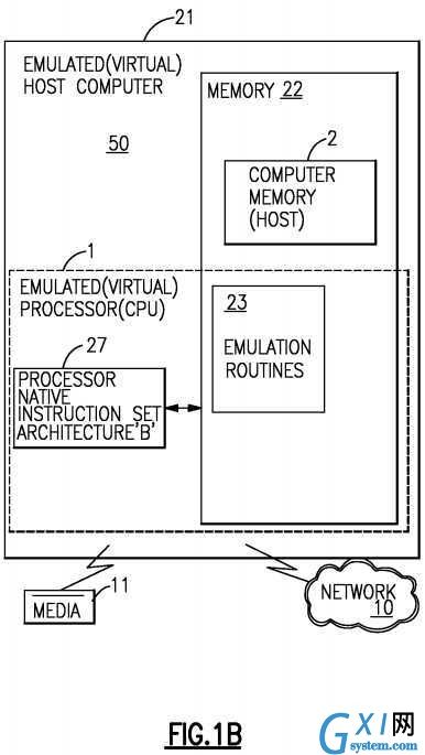
In?FIG. 1B, an embodiment of an emulated Host Computer system?21?is provided that emulates a Host computer system?50of a Host architecture. In the emulated Host Computer system?21, the Host processor (CPU)?1?is an emulated Host processor (or virtual Host processor) and comprises an emulation processor?27?having a different native instruction set architecture than that of the processor?1?of the Host Computer?50. The emulated Host Computer system?21?has memory?22accessible to the emulation processor?27. In the example embodiment, the Memory?22?is partitioned into a Host Computer Memory?2?portion and an Emulation Routines?23?portion. The Host Computer Memory?2?is available to programs of the emulated Host Computer?21?according to Host Computer Architecture. The emulation Processor?27?executes native instructions of an architected instruction set of an architecture other than that of the emulated processor?1, the native instructions obtained from Emulation Routines memory?23, and may access a Host instruction for execution from a program in Host Computer Memory?2?by employing one or more instruction(s) obtained in a Sequence & Access/Decode routine which may decode the Host instruction(s) accessed to determine a native instruction execution routine for emulating the function of the Host instruction accessed. Other facilities that are defined for the Host Computer System?50?architecture may be emulated by Architected Facilities Routines, including such facilities as General Purpose Registers, Control Registers, Dynamic Address Translation and I/O Subsystem support and processor cache for example. The Emulation Routines may also take advantage of function available in the emulation Processor?27?(such as general registers and dynamic translation of virtual addresses) to improve performance of the Emulation Routines. Special Hardware and Off-Load Engines may also be provided to assist the processor?27?in emulating the function of the Host Computer?50.
In a mainframe, architected machine instructions are used by programmers, for example by "C" programmers through a compiler application. These instructions stored in the storage medium may be executed natively in a mainframe server, or alternatively in machines executing other architectures. They can be emulated in the existing and in future mainframe servers and on other machines. They may be executed in machines running on operating systems, such as open source, on a wide variety of machines using hardware manufactured by various companies in an emulation mode. In emulation mode, emulation software is executed by a native processor to emulate the architecture of an emulated processor.
The native processor?27?typically executes emulation software?23?comprising either firmware or a native operating system to perform emulation of the emulated processor. The emulation software?23?is responsible for fetching and executing instructions of the emulated processor architecture. The emulation software?23?maintains an emulated program counter to keep track of instruction boundaries. The emulation software?23?may fetch one or more emulated machine instructions at a time and convert the one or more emulated machine instructions to a corresponding group of native machine instructions for execution by the native processor?27. These converted instructions may be cached such that a faster conversion can be accomplished. Not withstanding, the emulation software must maintain the architecture rules of the emulated processor architecture so as to assure operating systems and applications written for the emulated processor operate correctly. Furthermore the emulation software must provide resources identified by the emulated processor?1?architecture including, but not limited to control registers, general purpose registers, floating point registers, dynamic address translation function including segment tables and page tables for example, interrupt mechanisms, context switch mechanisms, Time of Day (TOD) clocks and architected interfaces to I/O subsystems such that an operating system or an application program designed to run on the emulated processor, can be run on the native processor having the emulation software.
A specific instruction being emulated is decoded, and a subroutine is called to perform the function of the individual instruction. An emulation software function?23?emulating a function of an emulated processor?1?is implemented, for example, in a "C" subroutine or driver, or some other method of providing a driver for the specific hardware as will be within the skill of those in the art after understanding the description of the preferred embodiment. Various software and hardware emulation patents including, but not limited to (1) U.S. Pat. No. 5,551,013 for a "Multiprocessor for hardware emulation" by Beausoleil et al.; (2) U.S. Pat. No. 6,009,261: "Preprocessing of stored target routines for emulating incompatible instructions on a target processor" by Scalzi et al; (3) U.S. Pat. No. 5,574,873: "Decoding guest instruction to directly access emulation routines that emulate the guest instructions" by Davidian et al; (4) U.S. Pat. No. 6,308,255: "Symmetrical multiprocessing bus and chipset used for coprocessor support allowing non-native code to run in a system" by Gorishek et al; (5) U.S. Pat. No. 6,463,582: "Dynamic optimizing object code translator for architecture emulation and dynamic optimizing object code translation method" by Lethin et al; (6) U.S. Pat. No. 5,790,825: "Method for emulating guest instructions on a host computer through dynamic recompilation of host instructions" by Eric Traut; and many others, illustrate the a variety of known ways to achieve emulation of an instruction format architected for a different machine for a target machine available to those skilled in the art, as well as those commercial software techniques used by those referenced above.
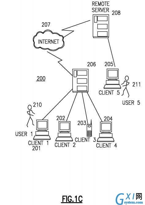
FIG. 1C?illustrates a data processing network?100?in which an embodiment may be practiced. The data processing network100?may include a plurality of individual networks, such as a wireless network and a wired network, each of which may include a plurality of individual workstations?101,?102,?103,?104,?105. Additionally, as those skilled in the art will appreciate, one or more LANs may be included, where a LAN may comprise a plurality of intelligent workstations coupled to a host processor.
Still referring to?FIG. 1, the networks may also include mainframe computers or servers, such as a gateway computer (client server?106) or application server (remote server?108?which may access a data repository and may also be accessed directly from a workstation?105). A gateway computer?106?serves as a point of entry into each network?107. A gateway is needed when connecting one networking protocol to another. The gateway?106?may be preferably coupled to another network (the Internet?107?for example) by means of a communications link. The gateway?106?may also be directly coupled to one or more workstations?101,?102,?103,?104?using a communications link.
U.S. Pat. No. 6,578,111, "Cache memory system and method for managing streaming-data", Jun. 10, 2003, incorporated by reference, describes a cache memory system as follows: A system and method are provided for efficient handling of streaming-data in a cache memory system having a cache with several cache-lines capable of storing data. In one aspect, a method is provided for determining before storing data to a cache-line if the storing of data will replace earlier data already stored in cache. If the storing of data will replace data in the cache, it is determined if the data that will be replaced is streaming-data. If the data to be replaced is not streaming-data, it is stored into victim cache. However, if the data to be replaced is streaming-data, it is not stored into the victim cache, thereby improving system efficiency by eliminating the copying of data to be replaced and avoiding replacing other earlier data in victim cache that may be needed in the future.
Modem computer systems generally include a central processing unit (CPU) or processor for processing data and a memory system for storing operating instructions and data. Typically, the speed at which the processor is able to decode and execute instructions to process data exceeds the speed at which instructions and data is transferred between the memory system and the processor. Thus, the processor is often forced to wait for the memory system to respond. One way of reducing this memory latency period is to organize computer memory into a memory hierarchy. A memory hierarchy consists of multiple levels of memory each using different devices for storing data and each having different speeds, capacities and cost associated therewith. Generally, the lowest-level of memory, commonly known as a cache, is coupled closely to the processor and uses relatively expensive, faster devices that make information, either data or instructions, available to the processor in a shorter period of time. The higher-levels typically include a main-memory and mass-data-storage devices that albeit larger are slower and are therefore correspondingly cheaper.
Use of a cache reduces the memory latency period by temporarily storing a small subset of data from higher-levels of the memory system. When the processor needs information for an application, it first checks the high-speed cache. If the information is found in the cache (known as a cache-hit), the information will be retrieved from the cache and execution of the application will resume. If the information is not found in the cache (known as a cache-miss) then the processor will proceed to access the slower, higher-level memories. Information accessed in the higher-level memories is simultaneously stored or written in the lower-level cache so that should the information be required again in the future it is obtained directly from the lower-level cache, thereby reducing or eliminating any memory latency period.
Similarly, use of a cache can reduce the memory latency period during a write operation by writing to the cache. This reduces the memory latency period in two ways. First, by enabling the processor to write at the much greater speed of the cache, and second by storing or loading the information in the cache so that, again, should the processor need the information in the future it is obtained directly from the cache.
There are three primary types of technology used in memories today. The main-memory is typically implemented using slower, cheaper dynamic random access memory (DRAM) devices. The cache is implemented using faster random access memory devices, such as static random access memory devices (SRAMs) so that accessing a cache takes much less time to complete than to access main-memory. SRAMs typically require greater number of devices per bit of information stored, and thus are more expensive than DRAM. In order to further reduce the memory latency period the cache may be located on the same chip as the CPU. The proximity of the cache to the CPU increases the speed with which the CPU can access the cache by eliminating delays due to transmission over external circuits. A cache located on the same chip as the CPU is often known as primary or level 1 (L1 cache) cache since the memory system typically includes a larger, slower level 2 (L2 cache) cache outside the CPU chip. Some memory systems include additional caches, for example a level (L3 cache) or victim cache for temporarily storing data displaced from the L2 cache.
As the name implies, at the highest-level in memory, mass-storage-devices provide the largest data storage capacity and typically use the slowest and therefore cheapest technology. For example, magnetic, optical or magnetic-optical technologies to store large amounts of instructions and data on tapes, or fixed or removable disks.
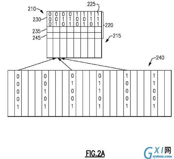
Referring to?FIG. 2A, cache?210?is divided logically into two main components or functional units. Data-store?215, where the cached information is actually stored, and tag-field?220, a small area of memory used by the cache to keep track of the location in the memory where the associated data can be found. The data-store is structured or organized as a number of cache-lines?225?or sets of cache-lines each having a tag-field?220?associated therewith, and each capable of storing multiple blocks or bytes of data. Typically, in modern computers each cache-line?225?may store 32 or 64 bytes of data. Each cache line is associated with a tag-field?220. In an n-way cache, there are n tags for each set. The tag-field?220?for each cache-line?225?includes an index?230?that uniquely identifies each cache-line or sets of cache-lines in the cache?210, and tag?235?that is used in combination with the index to identify an address in higher-level memory?240?from which data-stored in the cache-line has been read from or written to. Often the index?230?is not stored in the cache?210?but is implicit, with the address of the cache-line?225?itself providing the index. Typically, the tag-field?220?for each cache-line?225?also includes one or more bits, commonly known as a validity-bit?245, to indicate whether the cache-line contains valid data. In addition, the tag-field?220?may contain other bits (not shown) for example for indicating whether data at the location is dirty, that is has been modified but not written back to higher-level memory?240.
To speed up memory access operations, caches rely on principles of temporal and spatial-locality. These principles of locality are based on the assumption that, in general, a computer program accesses only a relatively small portion of the information available in computer memory in a given period of time. In particular, temporal locality holds that if some information is accessed once, it is likely to be accessed again soon, and spatial locality holds that if one memory location is accessed then other nearby memory locations are also likely to be accessed. Thus, in order to exploit temporal-locality, caches temporarily store information from a higher-level memory the first time it is accessed so that if it is accessed again soon it need not be retrieved from the higher-level memory. To exploit spatial-locality, caches transfer several blocks of data from contiguous addresses in higher-level memory, besides the requested block of data, each time data is written in the cache from higher-level memory.
The most important characteristics of a cache are its hit rate, that is the fraction of all memory accesses that are satisfied from the cache over a given period of time, and its access time, that is the time it takes to read from or write to the cache. These in turn depend in large part on how the cache is mapped to addresses in the higher-level memory. The choice of mapping technique is so critical to the design of the cache that the cache is often named after this choice. There are generally three different ways to map the cache to the addresses in memory.
Direct-mapping, shown in?FIG. 2A, is the simplest way to map a cache to addresses in main-memory. In the direct-mapping method the number of cache-lines is determined, the addresses in memory divided into the same number of groups of addresses, and addresses in each group associated with one cache-line. For example, for a cache having 2?n cache-lines, the addresses are divided into 2?n groups and each address in a group associated with a single cache-line. The lowest n address bits of an address corresponds to the index of the cache-line to which data from the address is stored. The remaining top address bits are stored as a tag that identifies from which of the several possible addresses in the group the data originated. For example, to map a 64 megabyte (MB) main-memory to a 512 kilobyte (KB) direct mapped cache having 16,384 cache-lines, each cache-line is shared by a group of 4,096 addresses in main-memory. To address 64-MB of memory requires 26 address bits since 64-MB is 2?26 bytes. The lowest five of these address bits, A0 to A4, are ignored in the mapping process, although the processor will use them later to determine which of the 32 bytes of data in the cache-line to accesses. The next 14 address bits, A5 to A18, provide the index of the cache-line to which the address is mapped. Because any cache-line can hold data from any one of 4,096 possible addresses in main-memory, the next seven highest address bits, A19 to A25, are used as a tag to identify to the processor which of the addresses the cache-line holds data from. This scheme, while simple, has the disadvantage that if the program alternately accesses different addresses which map to the same cache location, i.e., addresses within the same group, then it will suffer a cache-miss on every access to these locations.
A fully-associative mapped cache (not shown) avoids the cache conflict of the directly mapped cache by allowing blocks of data from any address in main-memory to be stored anywhere in the cache. However, one problem with fully associative caches is that the whole main-memory address must be used as a tag, thereby increasing the size of the tag-field and reducing cache capacity for storing data. Also, because the requested address must be compared simultaneously (associatively) with all tags in the cache, the access time for the cache is increased.
A 2-way set associative cache, shown in?FIG. 2B, is a compromise between the direct mapped and fully associative designs. In this design, the cache?210?is broken into sets?250?each having a number or ID, 2, 4, 8 etc., of cache-lines?225and each address in main-memory?240?is assigned to a set and is able to be stored in any one of the cache-lines within the set. Typically, such a cache is referred to as a n-way set associative cache where n is the number of cache-lines in each set.?FIG. 2B?shows an example of a 2-way set associative cache.
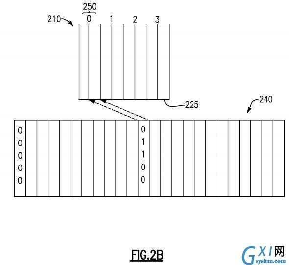
Memory addresses are mapped in the cache in a manner similar to the directly mapped cache. For example, to map a 64-MB main-memory having 26 address bits to a 512-KB 4-way set associative cache the cache is divided into 4,096 sets of 4 cache-lines each and 16,384 addresses in main-memory associated with each set. Address bits A5 to A16 of a memory address represent the index of the set to which the address maps to. The memory address could be mapped to any of the four cache-lines in the set. Because any cache-line within a set can hold data from any one of 16,384 possible memory addresses, the next nine highest address bits, A17 to A25, are used as a tag to identify to the processor which of the memory addresses the cache-line holds data from. Again, the lowest five address bits, A0 to A4, are ignored in the mapping process, although the processor will use them later to determine which of the 32 bytes of data in the cache-line to accesses.
When a fully associative or a set associative cache is full and it is desired to store another cache-line of data in the cache then a cache-line is selected to be written-back or flushed to main-memory or to a higher-level victim cache. The new data is then stored in place of the flushed cache-line. The cache-line to be flushed is chosen based on a replacement policy implemented via a replacement algorithm.
There are various different replacement algorithms that can be used. One utilized replacement algorithm is known as the Least Recently Used (LRU) replacement algorithm. According to the LRU replacement algorithm, for each cache-line, the cache controller maintains in a register several status bits that keep track of the number of times in which the cache-line was last accessed, a cache line state. Each time one of the cache-lines is accessed, it is marked most recently used (MRU) and the other cache-lines in the same set of cache-lines are adjusted accordingly. A cache-line is elected to be flushed if it has been accessed (read or written to) less recently than any other cache-line on the set of cache-lines, i.e. the LRU cache line. The LRU replacement policy is based on the assumption that, in general, the cache-line which has not been accessed for longest time is least likely to be accessed in the near future. For example, in an 8 way set associative cache, for each row of the cache the LRU logic tracks the order of recent usage of each of the 8 set ids.
Other replacement schemes that are used include random replacement, an algorithm that picks any cache-line with equal probability; First-In-First-Out (FIFO), an algorithm that simply replaces the first cache-line loaded in a particular set or group of cache lines; and Lease-Frequently-Used (LFU) algorithm that replace the least used cache line by counting (with an upper threshold) how often a cache line had been used.
Referring to?FIG. 3, an exemplary processor embodiment is depicted for processor?106. Typically one or more levels of Cache?303?are employed to buffer memory blocks in order to improve processor performance. The cache?303?is a high speed buffer holding cache lines of memory data that are likely to be used. Typical cache lines are 32, 64, 128 or 256 bytes of memory data. Separate Caches are often employed for caching instructions than for caching data. Cache coherence (synchronization of copies of lines in Memory and the Caches) among multiple processors is often provided by various "Snoop" algorithms well known in the art.
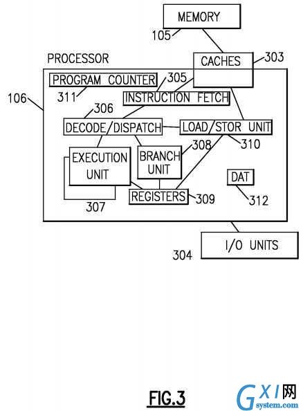
A program counter (instruction counter)?311?keeps track of the address of the current instruction to be executed. A program counter in a z/Architecture processor is 64 bits and can be truncated to 31 or 24 bits to support prior addressing limits. A program counter is typically embodied in a PSW (program status word) of a computer such that it persists during context switching. Thus, a program in progress, having a program counter value, may be interrupted by, for example, the operating system (context switch from the program environment to the Operating system environment). The PSW of the program maintains the program counter value while the program is not active, and the program counter (in the PSW) of the operating system is used while the operating system is executing. Typically the Program counter is incremented by an amount equal to the number of bytes of the current instruction. RISC (Reduced Instruction Set Computing) instructions are typically fixed length while CISC (Complex Instruction Set Computing) instructions are typically variable length. Instructions of the IBM z/Architecture are CISC instructions having a length of 2, 4 or 6 bytes. The Program counter?311?is modified by either a context switch operation or a Branch taken operation of a Branch instruction for example. In a context switch operation, the current program counter value is saved in a Program Status Word (PSW) along with other state information about the program being executed (such as condition codes), and a new program counter value is loaded pointing to an instruction of a new program module to be executed. A branch taken operation is performed in order to permit the program to make decisions or loop within the program by loading the result of the Branch Instruction into the Program Counter?311.
Typically an instruction Fetch Unit?305?is employed to fetch instructions on behalf of the processor?106. The fetch unit either fetches "next sequential instructions", target instructions of Branch Taken instructions, or first instructions of a program following a context switch. Modern Instruction fetch units often employ prefetch techniques to speculatively prefetch instructions based on the likelihood that the prefetched instructions might be used. For example, a fetch unit may fetch 16 bytes of instruction that includes the next sequential instruction and additional bytes of further sequential instructions.
The fetched instructions are then executed by the processor?106. In an embodiment, the fetched instruction(s) are passed to a dispatch unit?306?of the fetch unit. The dispatch unit decodes the instruction(s) and forwards information about the decoded instruction(s) to appropriate units?307?308?310. An execution unit?307?will typically receive information about decoded arithmetic instructions from the instruction fetch unit?305?and will perform arithmetic operations on operands according to the opcode of the instruction. Operands are provided to the execution unit?307?preferably either from memory105, architected registers?309?or from an immediate field of the instruction being executed. Results of the execution, when stored, are stored either in memory?105, registers?309?or in other machine hardware (such as control registers, PSW registers and the like).
A processor?106?typically has one or more execution units?307?308?310?for executing the function of the instruction. Referring to?FIG. 4A, an execution unit?307?may communicate with architected general registers?309, a decode/dispatch unit?306?a load store unit?310?and other?401?processor units by way of interfacing logic?407. An Execution unit?307?may employ several register circuits?403?404?405?to hold information that the arithmetic logic unit (ALU)?402?will operate on. The ALU performs arithmetic operations such as add, subtract, multiply and divide as well as logical function such as and, or and exclusive-or (xor), rotate and shift. Preferably the ALU supports specialized operations that are design dependent. Other circuits may provide other architected facilities?408?including condition codes and recovery support logic for example. Typically the result of an ALU operation is held in an output register circuit?406?which can forward the result to a variety of other processing functions. There are many arrangements of processor units, the present description is only intended to provide a representative understanding of one embodiment.
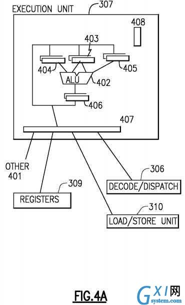
An ADD instruction for example would be executed in an execution unit?307?having arithmetic and logical functionality while a Floating Point instruction for example would be executed in a Floating Point Execution having specialized Floating Point capability. Preferably, an execution unit operates on operands identified by an instruction by performing an opcode defined function on the operands. For example, an ADD instruction may be executed by an execution unit?307?on operands found in two registers?309?identified by register fields of the instruction. The execution unit?307?performs the arithmetic addition on two operands and stores the result in a third operand where the third operand may be a third register or one of the two source registers.
Some ALUs?402?are designed for scalar operations and some for floating point. Data may be Big Endian (where the least significant byte is at the highest byte address) or Little Endian (where the least significant byte is at the lowest byte address) depending on architecture. The IBM z/Architecture is Big Endian. Signed fields may be sign and magnitude, 1‘s complement or 2‘s complement depending on architecture. A 2‘s complement number is advantageous in that the ALU does not need to design a subtract capability since either a negative value or a positive value in 2‘s complement requires only and addition within the ALU. Numbers are commonly described in shorthand, where a 12 bit field defines an address of a 4,096 byte block and is commonly described as a 4 Kbyte (Kilo-byte) block for example.
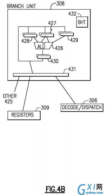
Referring to?FIG. 4B, Branch instruction information for executing a branch instruction is typically sent to a branch unit?308which often employs a branch prediction algorithm such as a branch history table?432?to predict the outcome of the branch before other conditional operations are complete. The target of the current branch instruction will be fetched and speculatively executed before the conditional operations are complete. When the conditional operations are completed the speculatively executed branch instructions are either completed or discarded based on the conditions of the conditional operation and the speculated outcome. A typical branch instruction may test condition codes and branch to a target address if the condition codes meet the branch requirement of the branch instruction, a target address may be calculated based on several numbers including ones found in register fields or an immediate field of the instruction for example. The branch unit308?may employ an ALU?426?having a plurality of input register circuits?427?428?429?and an output register circuit?430. The branch unit?308?may communicate with general registers?309, decode dispatch unit?306?or other circuits?425?for example.
The execution of a group of instructions can be interrupted for a variety of reasons including a context switch initiated by an operating system, a program exception or error causing a context switch, an I/O interruption signal causing a context switch or multi-threading activity of a plurality of programs (in a multi-threaded environment) for example. Preferably a context switch action saves state information about a currently executing program and then loads state information about another program being invoked. State information may be saved in hardware registers or in memory for example. State information preferably comprises a program counter value pointing to a next instruction to be executed, condition codes, memory translation information and architected register content. A context switch activity can be exercised by hardware circuits, application programs, operating system programs or firmware code (microcode, pico-code or licensed internal code (LIC) alone or in combination.
A processor accesses operands according to instruction defined methods. The instruction may provide an immediate operand using the value of a portion of the instruction, may provide one or more register fields explicitly pointing to either general purpose registers or special purpose registers (floating point registers for example). The instruction may utilize implied registers identified by an opcode field as operands. The instruction may utilize memory locations for operands. A memory location of an operand may be provided by a register, an immediate field, or a combination of registers and immediate field as exemplified by the z/Architecture long displacement facility wherein the instruction defines a Base register, an Index register and an immediate field (displacement field) that are added together to provide the address of the operand in memory for example. Location herein typically implies a location in main memory (main storage) unless otherwise indicated.
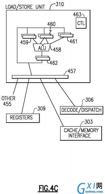
Referring to?FIG. 4C, a processor accesses storage using a Load/Store unit?310. The Load/Store unit?310?may perform a Load operation by obtaining the address of the target operand in memory?303?and loading the operand in a register?309?or another memory?303?location, or may perform a Store operation by obtaining the address of the target operand in memory303?and storing data obtained from a register?309?or another memory?303?location in the target operand location in memory303. The Load/Store unit?310?may be speculative and may access memory in a sequence that is out-of-order relative to instruction sequence, however the Load/Store unit?310?must maintain the appearance to programs that instructions were executed in order. A load/store unit?310?may communicate with general registers?309, decode/dispatch unit?306, Cache/Memory interface?303?or other elements?455?and comprises various register circuits, ALUs?458?and control logic?463to calculate storage addresses and to provide pipeline sequencing to keep operations in-order. Some operations may be out of order but the Load/Store unit provides functionality to make the out of order operations to appear to the program as having been performed in order as is well known in the art.
Preferably addresses that an application program "sees" are often referred to as virtual addresses. Virtual addresses are sometimes referred to as "logical addresses" and "effective addresses". These virtual addresses are virtual in that they are redirected to physical memory location by one of a variety of Dynamic Address Translation (DAT)?312?technologies including, but not limited to simply prefixing a virtual address with an offset value, translating the virtual address via one or more translation tables, the translation tables preferably comprising at least a segment table and a page table alone or in combination, preferably, the segment table having an entry pointing to the page table. In z/Architecture, a hierarchy of translation is provided including a region first table, a region second table, a region third table, a segment table and an optional page table. The performance of the address translation is often improved by utilizing a Translation Lookaside Buffer (TLB) which comprises entries mapping a virtual address to an associated physical memory location. The entries are created when DAT?312?translates a virtual address using the translation tables. Subsequent use of the virtual address can then utilize the entry of the fast TLB rather than the slow sequential Translation table accesses. TLB content may be managed by a variety of replacement algorithms including LRU (Least Recently used).
In the case where the Processor is a processor of a multi-processor system, each processor has responsibility to keep shared resources such as I/O, caches, TLBs and Memory interlocked for coherency. Typically "snoop" technologies will be utilized in maintaining cache coherency. In a snoop environment, each cache line may be marked as being in any one of a shared state, an exclusive state, a changed state, an invalid state and the like in order to facilitate sharing.
I/O units?304?provide the processor with means for attaching to peripheral devices including Tape, Disc, Printers, Displays, and networks for example. I/O units are often presented to the computer program by software Drivers. In Mainframes such as the z/Series from IBM. Channel Adapters and Open System Adapters are I/O units of the Mainframe that provide the communications between the operating system and peripheral devices.
The following description, in part from the "IBM z/Architecture Principles of Operation" published August 2010, reference number SA22-7832-08, describes an architectural view of a computer system:
- Storage:
A computer system includes information in main storage, as well as addressing, protection, and reference and change recording. Some aspects of addressing include the format of addresses, the concept of address spaces, the various types of addresses, and the manner in which one type of address is translated to another type of address. Some of main storage includes permanently assigned storage locations. Main storage provides the system with directly addressable fast-access storage of data. Both data and programs must be loaded into main storage (from input devices) before they can be processed.
Main storage may include one or more smaller, faster-access buffer storages, sometimes called caches. A cache is typically physically associated with a CPU or an I/O processor. The effects, except on performance, of the physical construction and use of distinct storage media are generally not observable by the program.
Separate caches may be maintained for instructions and for data operands. Information within a cache is maintained in contiguous bytes on an integral boundary called a cache block or cache line (or line, for short). A model may provide an EXTRACT CACHE ATTRIBUTE instruction which returns the size of a cache line in bytes. A model may also provide preFETCH DATA and preFETCH DATA RELATIVE LONG instructions which effect the prefetching of storage into the data or instruction cache or the releasing of data from the cache.
Storage is viewed as a long horizontal string of bits. For most operations, accesses to storage proceed in a left-to-right sequence. The string of bits is subdivided into units of eight bits. An eight-bit unit is called a byte, which is the basic building block of all information formats. Each byte location in storage is identified by a unique nonnegative integer, which is the address of that byte location or, simply, the byte address. Adjacent byte locations have consecutive addresses, starting with 0 on the left and proceeding in a left-to-right sequence. Addresses are unsigned binary integers and are 24, 31, or 64 bits.
Information is transmitted between storage and a CPU or a channel subsystem one byte, or a group of bytes, at a time. Unless otherwise specified, a group of bytes in storage is addressed by the leftmost byte of the group. The number of bytes in the group is either implied or explicitly specified by the operation to be performed. When used in a CPU operation, a group of bytes is called a field. Within each group of bytes, bits are numbered in a left-to-right sequence. The leftmost bits are sometimes referred to as the "high-order" bits and the rightmost bits as the "low-order" bits. Bit numbers are not storage addresses, however. Only bytes can be addressed. To operate on individual bits of a byte in storage, it is necessary to access the entire byte. The bits in a byte are numbered 0 through 7, from left to right. The bits in an address may be numbered 8-31 or 40-63 for 24-bit addresses or 1-31 or 33-63 for 31-bit addresses; they are numbered 0-63 for 64-bit addresses. Within any other fixed-length format of multiple bytes, the bits making up the format are consecutively numbered starting from 0. For purposes of error detection, and in preferably for correction, one or more check bits may be transmitted with each byte or with a group of bytes. Such check bits are generated automatically by the machine and cannot be directly controlled by the program. Storage capacities are expressed in number of bytes. When the length of a storage-operand field is implied by the operation code of an instruction, the field is said to have a fixed length, which can be one, two, four, eight, or sixteen bytes. Larger fields may be implied for some instructions. When the length of a storage-operand field is not implied but is stated explicitly, the field is said to have a variable length. Variable-length operands can vary in length by increments of one byte. When information is placed in storage, the contents of only those byte locations are replaced that are included in the designated field, even though the width of the physical path to storage may be greater than the length of the field being stored.
Certain units of information must be on an integral boundary in storage. A boundary is called integral for a unit of information when its storage address is a multiple of the length of the unit in bytes. Special names are given to fields of 2, 4, 8, and 16 bytes on an integral boundary. A halfword is a group of two consecutive bytes on a two-byte boundary and is the basic building block of instructions. A word is a group of four consecutive bytes on a four-byte boundary. A doubleword is a group of eight consecutive bytes on an eight-byte boundary. A quadword is a group of 16 consecutive bytes on a 16-byte boundary. When storage addresses designate halfwords, words, doublewords, and quadwords, the binary representation of the address contains one, two, three, or four rightmost zero bits, respectively. Instructions must be on two-byte integral boundaries. The storage operands of most instructions do not have boundary-alignment requirements.
On models that implement separate caches for instructions and data operands, a significant delay may be experienced if the program stores into a cache line from which instructions are subsequently fetched, regardless of whether the store alters the instructions that are subsequently fetched.
- Instructions:
Typically, operation of the CPU is controlled by instructions in storage that are executed sequentially, one at a time, left to right in an ascending sequence of storage addresses. A change in the sequential operation may be caused by branching, LOAD PSW, interruptions, SIGNAL PROCESSOR orders, or manual intervention.
Preferably an instruction comprises two major parts:
An operation code (op code), which specifies the operation to be performed
Optionally, the designation of the operands that participate.
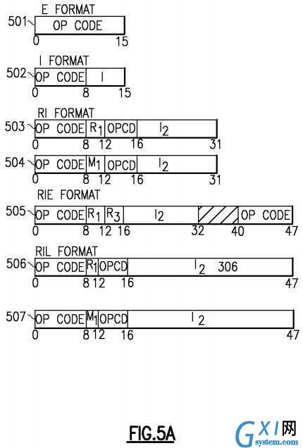
Instruction formats of the z/Architecture are shown in?FIGS. 5A-5F. An instruction can simply provide an Opcode?501, or an opcode and a variety of fields including immediate operands or register specifiers for locating operands in registers or in memory. The Opcode can indicate to the hardware that implied resources (operands etc.) are to be used such as one or more specific general purpose registers (GPRs). Operands can be grouped in three classes: operands located in registers, immediate operands, and operands in storage. Operands may be either explicitly or implicitly designated. Register operands can be located in general, floating-point, access, or control registers, with the type of register identified by the op code. The register containing the operand is specified by identifying the register in a four-bit field, called the R field, in the instruction. For some instructions, an operand is located in an implicitly designated register, the register being implied by the op code. Immediate operands are contained within the instruction, and the 8-bit, 16-bit, or 32-bit field containing the immediate operand is called the I field. Operands in storage may have an implied length; be specified by a bit mask: be specified by a four-bit or eight-bit length specification, called the L field, in the instruction; or have a length specified by the contents of a general register. The addresses of operands in storage are specified by means of a format that uses the contents of a general register as part of the address. This makes it possible to:
- 1. Specify a complete address by using an abbreviated notation.
- 2. Perform address manipulation using instructions which employ general registers for operands.
- 3. Modify addresses by program means without alteration of the instruction stream.
- 4. Operate independent of the location of data areas by directly using addresses received from other programs.
The address used to refer to storage either is contained in a register designated by the R field in the instruction or is calculated from a base address, index, and displacement, specified by the B, X, and D fields, respectively, in the instruction. When the CPU is in the access-register mode, a B or R field may designate an access register in addition to being used to specify an address. To describe the execution of instructions, operands are preferably designated as first and second operands and, in some cases, third and fourth operands. In general, two operands participate in an instruction execution, and the result replaces the first operand.
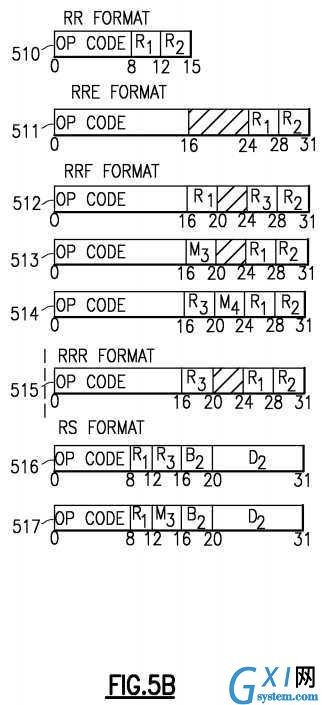
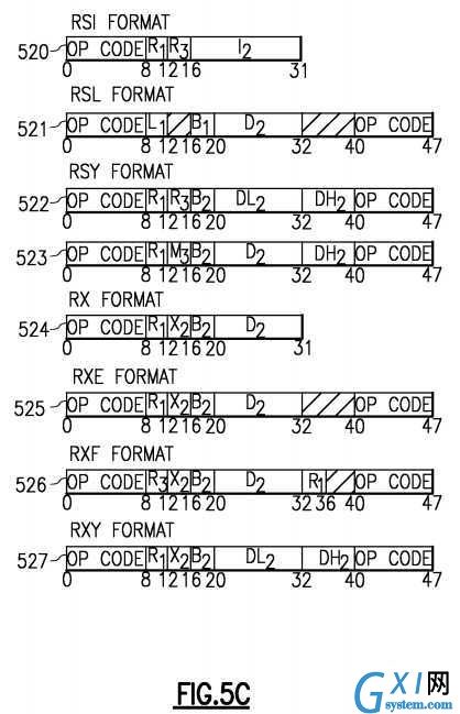
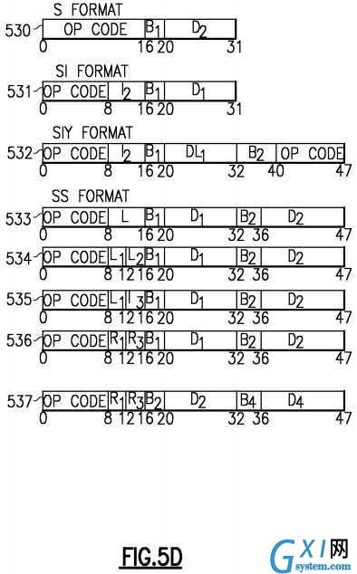
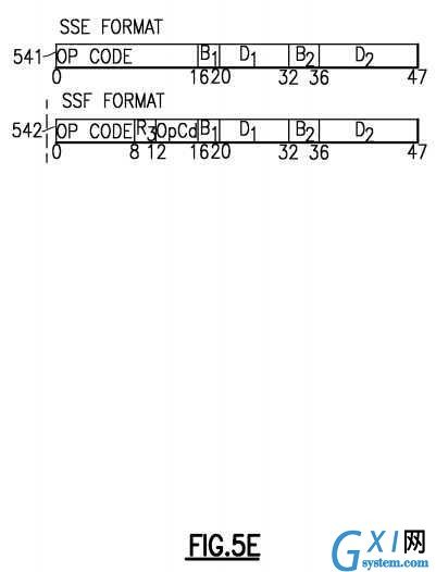
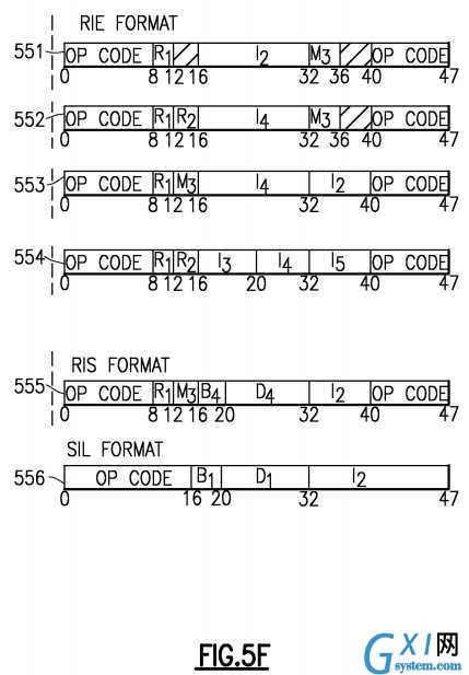
An instruction is one, two, or three halfwords in length and must be located in storage on a halfword boundary. Referring toFIGS. 5A-5F?depicting instruction formats, each instruction is in one of 25 basic formats: E?501, I?502, RI?503?504, RIE?505551?552?553?554, RIL?506?507, RIS?555, RR?510, RRE?511, RRF?512?513?514, RRS, RS?516?517, RSI?520, RSL?521, RSY?522?523, RX?524, RXE?525, RXF?526, RXY?527, S?530, SI?531, SIL?556, SIY?532, SS?533?534?535?536?537, SSE541?and SSF?542, with three variations of RRF, two of RI, RIL, RS, and RSY, five of RIE and SS.
The format names indicate, in general terms, the classes of operands which participate in the operation and some details about fields:
RIS denotes a register-and-immediate operation and a storage operation.
RRS denotes a register-and-register operation and a storage operation.
SIL denotes a storage-and-immediate operation, with a 16-bit immediate field.
In the I, RR, RS, RSI, RX, SI, and SS formats, the first byte of an instruction contains the op code. In the E, RRE, RRF, S, SIL, and SSE formats, the first two bytes of an instruction contain the op code, except that for some instructions in the S format, the op code is in only the first byte. In the RI and RIL formats, the op code is in the first byte and bit positions 12-15 of an instruction. In the RIE, RIS, RRS, RSL, RSY, RXE, RXF, RXY, and SIY formats, the op code is in the first byte and the sixth byte of an instruction. The first two bits of the first or only byte of the op code specify the length and format of the instruction, as follows:
In the RR, RRE, RRF, RRR, RX, RXE, RXF, RXY, RS, RSY, RSI, RI, RIE, and RIL formats, the contents of the register designated by the R1?field are called the first operand. The register containing the first operand is sometimes referred to as the "first operand location," and sometimes as "register R1". In the RR, RRE, RRF and RRR formats, the R2?field designates the register containing the second operand, and the R2?field may designate the same register as R1. In the RRF, RXF, RS, RSY, RSI, and RIE formats, the use of the R3?field depends on the instruction. In the RS and RSY formats, the R3?field may instead be an M3?field specifying a mask. The R field designates a general or access register in the general instructions, a general register in the control instructions, and a floating-point register or a general register in the floating-point instructions. For general and control registers, the register operand is in bit positions 32-63 of the 64-bit register or occupies the entire register, depending on the instruction.
In the I format, the contents of the eight-bit immediate-data field, the I field of the instruction, are directly used as the operand. In the SI format, the contents of the eight-bit immediate-data field, the I2?field of the instruction, are used directly as the second operand. The B1?and D1?fields specify the first operand, which is one byte in length. In the SIY format, the operation is the same except that DH1?and DL1?fields are used instead of a D1?field. In the RI format for the instructions ADD HALFWORD IMMEDIATE, COMPARE HALFWORD IMMEDIATE, LOAD HALFWORD IMMEDIATE, and MULTIPLY HALFWORD IMMEDIATE, the contents of the 16-bit I2?field of the instruction are used directly as a signed binary integer, and the R1?field specifies the first operand, which is 32 or 64 bits in length, depending on the instruction. For the instruction TEST UNDER MASK (TMHH, TMHL, TMLH, TMLL), the contents of the I2?field are used as a mask, and the R1?field specifies the first operand, which is 64 bits in length.
For the instructions INSERT IMMEDIATE, AND IMMEDIATE, OR IMMEDIATE, and LOAD LOGICAL IMMEDIATE, the contents of the I2?field are used as an unsigned binary integer or a logical value, and the R1?field specifies the first operand, which is 64 bits in length. For the relative-branch instructions in the RI and RSI formats, the contents of the 16-bit I2?field are used as a signed binary integer designating a number of halfwords. This number, when added to the address of the branch instruction, specifies the branch address. For relative-branch instructions in the RIL format, the I2?field is 32 bits and is used in the same way.
For the relative-branch instructions in the RI and RSI formats, the contents of the 16-bit I2?field are used as a signed binary integer designating a number of halfwords. This number, when added to the address of the branch instruction, specifies the branch address. For relative-branch instructions in the RIL format, the I2?field is 32 bits and is used in the same way. For the RIE-format instructions COMPARE IMMEDIATE AND BRANCH RELATIVE and COMPARE LOGICAL IMMEDIATE AND BRANCH RELATIVE, the contents of the 8-bit I2?field is used directly as the second operand. For the RIE-format instructions COMPARE IMMEDIATE AND BRANCH, COMPARE IMMEDIATE AND TRAP, COMPARE LOGICAL IMMEDIATE AND BRANCH, and COMPARE LOGICAL IMMEDIATE AND TRAP, the contents of the 16-bit I2?field are used directly as the second operand. For the RIE-format instructions COMPARE AND BRANCH RELATIVE, COMPARE IMMEDIATE AND BRANCH RELATIVE, COMPARE LOGICAL AND BRANCH RELATIVE, and COMPARE LOGICAL IMMEDIATE AND BRANCH RELATIVE, the contents of the 16-bit I4 field are used as a signed binary integer designating a number of halfwords that are added to the address of the instruction to form the branch address.
For the RIL-format instructions ADD IMMEDIATE, ADD LOGICAL IMMEDIATE, ADD LOGICAL WITH SIGNED IMMEDIATE, COMPARE IMMEDIATE, COMPARE LOGICAL IMMEDIATE, LOAD IMMEDIATE, and MULTIPLY SINGLE IMMEDIATE, the contents of the 32-bit I2?field are used directly as a the second operand.
For the RIS-format instructions, the contents of the 8-bit I2?field are used directly as the second operand. In the SIL format, the contents of the 16-bit I2?field are used directly as the second operand. The B1?and D1?fields specify the first operand, as described below.
In the RSL, SI, SIL, SSE, and most SS formats, the contents of the general register designated by the B1?field are added to the contents of the D1?field to form the first-operand address. In the RS, RSY, S, SIY, SS, and SSE formats, the contents of the general register designated by the B2?field are added to the contents of the D2?field or DH2?and DL2?fields to form the second-operand address. In the RX, RXE, RXF, and RXY formats, the contents of the general registers designated by the X2?and B2?fields are added to the contents of the D2?field or DH2?and DL2?fields to form the second-operand address. In the RIS and RRS formats, and in one SS format, the contents of the general register designated by the B4?field are added to the contents of the D4?field to form the fourth-operand address.
In the SS format with a single, eight-bit length field, for the instructions AND (NC), EXCLUSIVE OR (XC), MOVE (MVC), MOVE NUMERICS, MOVE ZONES, and OR (OC), L specifies the number of additional operand bytes to the right of the byte designated by the first-operand address. Therefore, the length in bytes of the first operand is 1-256, corresponding to a length code in L of 0-255. Storage results replace the first operand and are never stored outside the field specified by the address and length. In this format, the second operand has the same length as the first operand. There are variations of the preceding definition that apply to EDIT, EDIT AND MARK, PACK ASCII, PACK UNIcode, TRANSLATE. TRANSLATE AND TEST, UNPACK ASCII, and UNPACK UNIcode.
In the SS format with two length fields, and in the RSL format, L1?specifies the number of additional operand bytes to the right of the byte designated by the first-operand address. Therefore, the length in bytes of the first operand is 1-16, corresponding to a length code in L1?of 0-15. Similarly, L2?specifies the number of additional operand bytes to the right of the location designated by the second-operand address Results replace the first operand and are never stored outside the field specified by the address and length. If the first operand is longer than the second, the second operand is extended on the left with zeros up to the length of the first operand. This extension does not modify the second operand in storage. In the SS format with two R fields, as used by the MOVE TO PRIMARY, MOVE TO SECONDARY, and MOVE WITH KEY instructions, the contents of the general register specified by the R1?field are a 32-bit unsigned value called the true length. The operands are both of a length called the effective length. The effective length is equal to the true length or 256, whichever is less. The instructions set the condition code to facilitate programming a loop to move the total number of bytes specified by the true length. The SS format with two R fields is also used to specify a range of registers and two storage operands for the LOAD MULTIPLE DISJOINT instruction and to specify one or two registers and one or two storage operands for the PERFORM LOCKED OPERATION instruction.
A zero in any of the B1, B2, X2, or B4?fields indicates the absence of the corresponding address component. For the absent component, a zero is used informing the intermediate sum, regardless of the contents of general register 0. A displacement of zero has no special significance.
Bits 31 and 32 of the current PSW are the addressing-mode bits. Bit 31 is the extended-addressing mode bit, and bit 32 is the basic-addr


热门排行
今日推荐
-
ccleaner专业版

版本:v23.20.0
大小:40.18MB
日期:2024-09-29
-
draft.art手机版

版本:v1.0
大小:327KB
日期:2024-09-29
-
内蒙古特产网免费版

版本:v1.3
大小:2.94MB
日期:2024-09-29
-
乐走计步赚钱正版

版本:v1.3.0
大小:6.74MB
日期:2024-09-29
-
意见ai绘画免费版

版本:v1.0.0
大小:3.39MB
日期:2024-09-29
-
小红莓直播免费版

版本:1.0.4
大小:72.2 MB
日期:2024-09-29


